SOAK EGYPT in prayers
…an ecumenical prayer initiative for Egypt’s villages, towns, and cities.


Vision & Mission
Through collective and persistent prayer, to see multiplied churches planted and believers worshipping Christ all over Egypt.

GET INVOLVED
To soak Egypt in prayer by enlisting individuals, teams of believers, and churches who commit to spiritually adopt a village, town, or city in persistent, faith-filled prayer, at least once a week.
PRAYER FOCUS
That by His sovereign power, the Lord will bless and unite the Church in Egypt, and pave a way for His Church to exist in every village, town, and city in Egypt.
A COLLABORATIVE PRAYER INITIATIVE, NOT A PROJECT!
SOAK EGYPT is a collaborative and ecumenical evangelical prayer initiative with one objective: to see the Church of Egypt grow. We hear God calling the existing Church in Egypt and His global Church to adopt every village, town, and city of Egypt for prayer in 2023. The growth of the Church in Egypt will only happen as God’s people pray!
January to December 2023
Day(s)
:
Hour(s)
:
Minute(s)
:
Second(s)
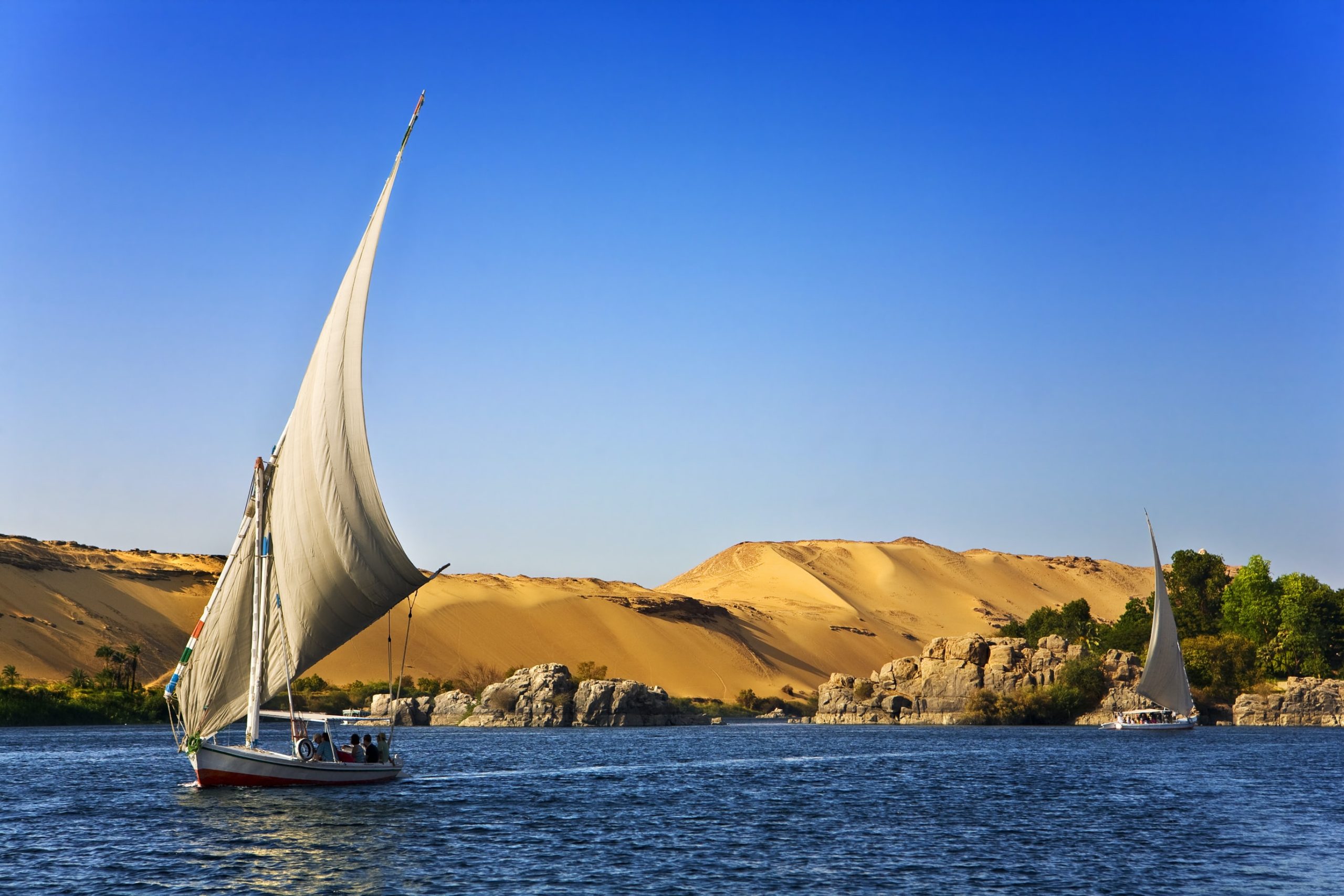
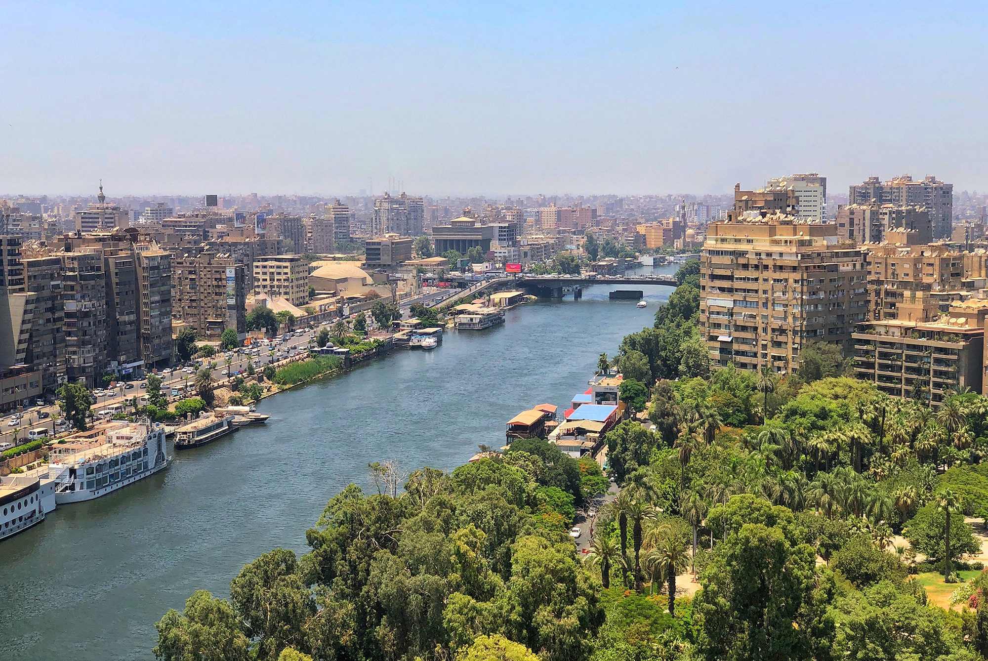
EGYPT, the beautiful land on the Nile!
Egypt is an open society, a tourist hub, and a welcoming country. For those yet to visit, Egypt is the land of a thousand treasures and destinations – the land of the Pharaohs, the Pyramids, the Nile, the Red Sea, the Mediterranean – and much more! And Egyptian hospitality is second to none. Welcome to Egypt – visit, play, and pray!
The Challenge
While the exact number is uncertain, there are hundreds of communities that need churches in Egypt. The Lord loves Egypt, and the Bible has bountiful promises about Egypt. Thankfully, Egypt permits Christians to gather and worship, and we need to ask the Lord to open the doors to make this happen.
GODS PROPHETIC WORD
Isaiah 19:19-23In that day there will be an altar to the LORD in the midst of the land of Egypt, and a pillar to the LORD at its border. And it will be for a sign and for a witness to the LORD of hosts in the land of Egypt; for they will cry to the LORD because of the oppressors, and He will send them a Savior and a Mighty One, and He will deliver them. Then the LORD will be known to Egypt, and the Egyptians will know the LORD in that day, and will make sacrifice and offering; yes, they will make a vow to the LORD and perform it. And the LORD will strike Egypt, He will strike and heal it; they will return to the LORD, and He will be entreated by them and heal them. In that day there will be a highway from Egypt to Assyria, and the Assyrian will come into Egypt and the Egyptian into Assyria, and the Egyptians will serve with the Assyrians.